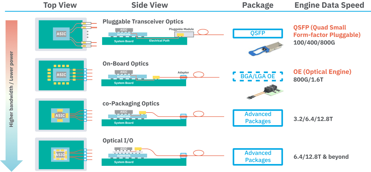
In traditional switch hardware, data is sent over optical fibre using pluggable transceiver modules (SFP, QSFP, etc.) that slot into cages on the switch faceplate. These modules convert electrical signals from the switch ASIC into light and back, with each link carrying tens or hundreds of gigabits per second. Co-packaged optics (CPO) changes this paradigm by moving the photonic engines into the switch package itself. In a co-packaged design, the laser diodes, modulators and detectors are integrated on or beside the switch chip (often on a silicon photonics engine) so that the high-speed SerDes signals only travel millimetres rather than centimetres on a PCB. In short, instead of having separate QSFP/QSFP-DD modules on the front panel, the optical I/O is built into the package. As Intel explains, placing the optics “near the switch within the same package” drastically reduces the electrical path and saves power. This contrasts with the conventional pluggable model (see above): each cage on the switch front panel contains a complete transceiver, and an electrical trace carries the signal to the ASIC across the board.
Pluggable optics have dominated for decades because they’re modular and low‐cost in volume. Standards like SFP+, QSFP+, QSFP28, QSFP56 and QSFP-DD let operators mix copper DACs, short-range fibre or long-range optics on a single switch. This modularity drove prices down. However, that flexibility now comes at a cost: power, heat and signal integrity. A pluggable module must house lasers, drivers, receivers and often DSP, all of which consume several watts each. For example, modern 400G modules typically draw 7–12 W per port, and 800G modules about 16–18 W. When a switch has dozens of ports, the power adds up to kilowatts just for optics. Moreover, each electrical lane (now up to 112 Gb/s or more) over the backplane or midplane suffers loss and crosstalk, requiring complex equalisation. In practice, engineers have observed that at 400GbE speeds and beyond “current pluggable optic technology no longer scales” – it simply cannot provide the necessary performance, power efficiency or density.
The Drive to Ever Higher Speeds
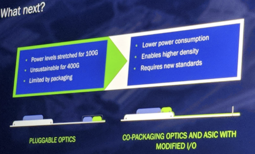
Data‐centre traffic is exploding, much of it in machine learning and HPC applications. At the same time, switch ASIC bandwidths have soared – modern silicon went from ~0.64 Tb/s in 2010 to over 51.2 Tb/s by 2022. For example, a 51.2 Tb/s switch has 512×100 Gb/s SerDes, which could be wired as 128×400G Ethernet ports. Pushing further to 102.4 Tb/s requires 512 lanes at 200 Gb/s (driving 800G or 1.6T interfaces). Each doubling of lane rate (e.g. from 100 Gb/s to 200 Gb/s) drastically shortens how far a signal can go over copper: at 200 Gb/s a passive copper link only reaches ~1 m. In other words, traditional copper interconnects become infeasible even for in-rack links. All this has hyper-scale operators (Facebook/Meta, Google, Microsoft, etc.) screaming that pluggable optics will not meet their needs. In fact, Facebook was already arguing in 2018 that by the 400GbE generation pluggable optics were “unsustainable” and co-packaging was the future. The slide below, from a Facebook networking presentation, encapsulates the problem: pluggable optics “power levels [are] stretched” for 100G and become “unsustainable for 400G”, whereas a co-packaged design promises “lower power consumption” and “higher density” of ports.
These issues – power, heat, density and signal integrity – are the technical drivers pushing the industry toward CPO. For instance, industry analysts note that at 51.2 Tb/s switch bandwidth, pluggable optics become “increasingly incompetent” due to limited panel space and long trace losses. Co-packaging removes the faceplate as a bottleneck. By “dissolving the module” and co-packaging the optics with the ASIC, the electrical SerDes channels shrink to millimetre‐scale lengths inside the package. This in-package link has much lower loss, greatly easing the SerDes design and cutting the required transmitter equalisation and power. In other words, instead of pushing a 100–200 Gb/s signal 50 cm over FR4, it only travels a few millimetres to an on-package photonic engine. The result is dramatically lower SerDes power per bit. In a mature analysis, Intel predicts that placing optics on-package “reduces power” and enables continuing scaling of switch bandwidth.
Silicon Photonics as the Enabler
What makes co-packaged optics practical is silicon photonics – photonic integrated circuits (PICs) built with CMOS (Complementary metal–oxide–semiconductor - https://en.wikipedia.org/wiki/CMOS) techniques. Silicon photonics allows lasers, modulators and detectors to be fabricated on silicon chips and co-packaged with the switch ASIC. In Intel’s demonstrator, each “photonic engine” was a 1.6 Tb/s array (four 400G channels) built on Intel’s silicon photonics platform. These engines include on-chip lasers and modulators, just like a tiny 4×100G transceiver built into the package. In effect, the discrete QSFP module is replaced by a silicon chiplet. This chip-scale approach brings the economies of scale of CMOS to optics – indeed, Intel points out they’ve already shipped millions of 100G silicon-photonics pluggables, and are now ramping 200/400G devices. Silicon photonics not only fits small enough to co-package, it also offers the performance needed at 50–200 Gb/s lane rates. Research labs (e.g. IBM) are even exploring polymer waveguides and novel packaging to couple many fibres at the die edge, boosting “beachfront density” by 6×. All these advances mean we can finally bring light directly to the switch ASIC, instead of a foot away on the faceplate.
Bonus: watch this excellent video at YouTube by Asianometry on Silicon Photonics. https://www.youtube.com/watch?v=29aTqLvRia8
Implications for Data Centres and AI
Data centres – especially those running AI/ML workloads – will feel the impact of co-packaging first. Modern AI training clusters move petabits of data between GPUs and servers every second. The demand for switch bandwidth in these systems is enormous and growing. Industry analysts warn that if network efficiency does not improve, data centres could consume vastly more power in the AI era. For example, a US DOE report cited in a recent industry article estimated that data-centre electricity use could triple (to ~12% of national power) by 2028 if nothing changes. Co-packaged optics can directly address this by slashing the power per bit. Early results suggest that switching from electrical backplanes to on-chip optics can “slash energy costs” for AI model training. Likewise, a recent blog notes that CPO lets system architects build much bigger “scale-up” clusters: instead of servers with 4–8 GPUs, future racks might have hundreds of co-packaged GPUs networked optically, achieving unprecedented bandwidth at lower power. In short, any application that requires huge aggregate throughput (large language model training, big HPC problems, etc.) will benefit most from co-packaged optics. Hyperscale cloud providers and supercomputing sites are thus the prime early adopters.
Benefits: Power, Density and More
The advantages of co-packaged optics are multifold. First and foremost is power. By eliminating the long PCB trace and bulky driver/DSP in a pluggable module, CPO drastically cuts the electrical link power. Intel and Broadcom both highlight that co-pack solutions achieve “industry-leading power efficiency and density”. In practice, moving the laser and electronics on-package can halve or better the power per port. A Broadcom press release emphasised that their 100G/lane co-pack line already delivers “the lowest power optical interconnects in the industry”, and their new 200G/lane gen will push that even further.
Density is another clear win. On a switch faceplate, there are only so many module cages one can fit. Co-packaging breaks that limit. The front-panel density of fibre (fibre strands per millimetre) becomes the new metric. For example, the OIF’s 3.2 Tb/s CPO standard specifies an edge-density of ~140 Tb/s per millimetre, far beyond what QSFP cages could ever manage. In practical terms, this means dozens of 800G or 1.6T ports can be packaged in the space of a few QSFP slots. This high port count is crucial for large switches in hyperscale networks.
Reliability and cooling also improve. With no hot-pluggable module hanging off the board, the system airflow is less obstructed. Co-pack engines can sit under a unified heatsink or coldplate, and the cooling requirements are more predictable. Intel notes that integrating photonics onto silicon dramatically improved field reliability of their optical links – a likely benefit of having solid-state laser engines instead of separate modules and connectors. Finally, because all ports use the same silicon-photonics type, inventory is simpler (at the cost of some flexibility). Of course, this also means lost serviceability: an APNIC guest post rightly warns that if a co-pack engine fails, it is not user-replaceable and mixing optics types is harder. In practice, hyperscale operators will trade off this inconvenience for the gains in power and performance.
Practical Demonstrations
Several industry demos have showcased co-packaged optics (CPO). In 2020, Intel quietly demonstrated a switch combining a Barefoot (now Intel) Tofino2 ASIC with co-packaged silicon photonic engines. In that prototype, four 1.6 Tb/s photonic engine dies were mounted around the Tofino chip on a multi-die package, yielding a 6.4 Tb/s switch. Fibers from each engine were routed inside the chassis to the front-panel MTP connectors. This setup resulted in much shorter electrical paths and eliminated the need for a front-plate heat sink above the ASIC. Intel even retained a few standard QSFP cages on the board for flexibility.
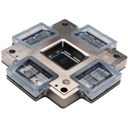
Broadcom, too, now ships co-packaged switches. Their 2024 “Bailly” Tomahawk-5 chip integrates eight optical engines (8×6.4 Tb/s) in-package for a total of 51.2 Tb/s. The photo above (from Broadcom/partners) shows such a package: the metal block holds the ASIC, and the four transparent hoods are the on-chip photonic engines. Broadcom’s press release confirms that their first-generation (100G-lane) CPO solutions are in volume use today, and they have announced a 200G-per-lane third generation. Indeed, they plan a 400G-per-lane future, underscoring how CPO is poised for the next wave of AI-scale networks.
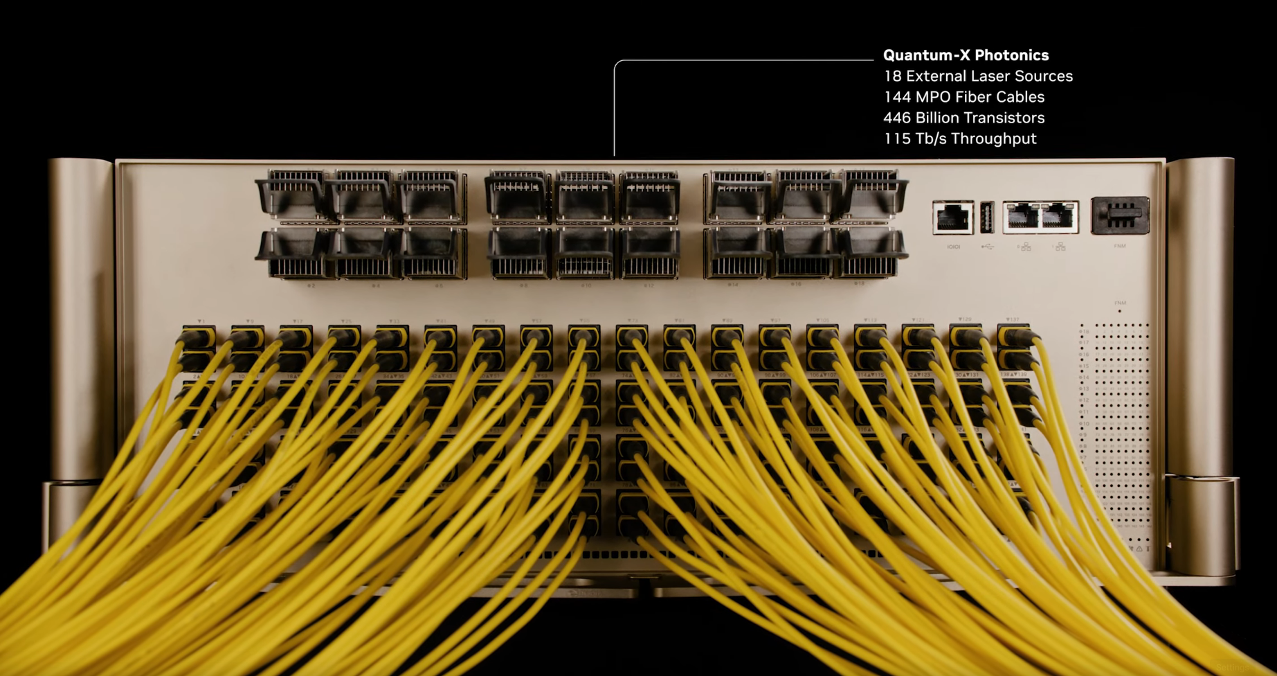
Other examples abound. Marvell announced in 2025 that its custom AI accelerator chips will adopt co-packaged optics, using a 6.4 Tb/s silicon-photonic engine to connect many GPUs or DPUs in a rack. Nvidia has also shown CPO concepts for its “Quantum-X” and “Spectrum-X” switches at recent conferences. Even the OIF has published a 3.2 Tb/s co-packaging module specification. These real-world developments make it clear: co-packaged optics is moving from research into products.
Deployment Outlook: When and Who
So when will co-pack optics actually arrive in data centres? The honest answer is: not overnight. We should expect a gradual rollout, starting with hyperscale and specialized HPC/AI environments. Early products (like Broadcom’s first CPO switches) are already here in 2024–25, but adoption requires new switch architectures, cabling and standards. Broadcom’s roadmap suggests 100G-lane CPO is mature, 200G-lane is emerging, and 400G-lane versions are being developed. Industry forecasts (LightCounting) predict shipments of CPO ports to climb from tiny today to tens of millions by 2029.
Who gains most? Clearly the mega-clouds, big AI companies and national supercomputing centres. They operate at scales (tens of thousands of switches, hundreds of thousands of servers) where even a small drop in power per bit translates to huge savings. They also build custom hardware where integrating co-packaged optics makes sense. For a large enterprise or smaller datacentre running mainly 10–100G, pluggable optics will still be dominant for some years. In fact, some network architects point out that alternate approaches – like “linear pluggable optics” (LPO), which minimise on-module DSP – might suffice in the near term. These experts caution that co-packaging sacrifices the flexibility of hot-pluggable modules and complicates servicing.
Conclusion
Co-packaged optics is a deep architectural shift driven by the limits of pluggable modules at very high speeds. By bringing optical engines on-package via silicon photonics, we can achieve far higher link densities and far lower power per bit. The transition is already underway in leading labs and products – from Intel’s Tofino2 demo to Broadcom’s switch ASICs and Marvell’s AI engines. While it won’t replace pluggables everywhere immediately, CPO is becoming essential for the next generation of AI and cloud networks.
References
- Hands-on with the Intel Co-Packaged Optics and Silicon Photonics Switch
- Co-packaged optics (CPO): status, challenges, and solutions - PMC
- Intel Demonstrates Industry-First Co-Packaged Optics Ethernet Switch
- Arista 400G Transceivers and Cables: Q&A
- Arista 800G Transceivers and Cables: Q&A
- Key Challenges and Innovations for 800G and 1.6T Networking
- Next Up for Custom AI Accelerators: Co-Packaged Optics
- Co-packaged optics can supercharge generative AI computing - IBM Research
- Broadcom Announces Third-Generation Co-Packaged Optics
- OIF Launches the Industry’s First Co-Packaging Standard
- Co-Packaged Optics — a deep dive | APNIC Blog